Scientific activity area:
The team's scientific interests include: development of technologies for the production of selected semiconductor devices and microelectronic structures based on silicon and silicon carbide, the use of laser techniques for structuring of semiconductor materials, diagnostics and analysis of the functional properties of microelectronic materials and structures and research in the area of integrated Lab-on-Chip structures.
Current research topics:
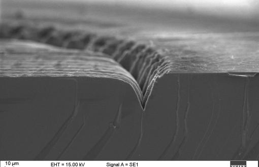
- application of laser techniques in the processes of electrical contacts fabrication for SiC-based power devices,
- realization of silicon- and silicon carbide-based discrete power semiconductor devices,
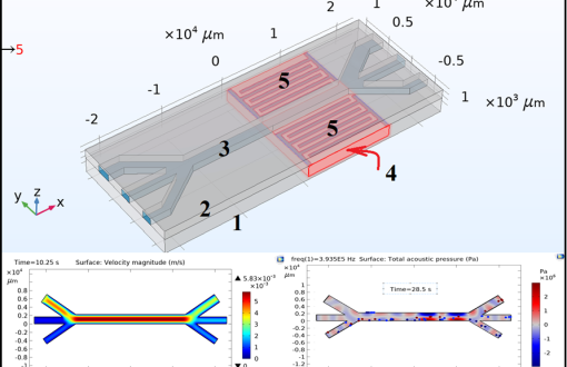
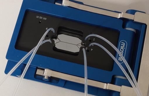
- design and analysis of integrated Lab-On-Chip structures,
- advanced characterization of electrical parameters (I-V characteristics, Hall voltages), surface morphology (optical and electron microscopy, surface profilometry) and structural analysis (EDS - energy dispersive spectroscopy, ellipsometry).
Research facilities:
The team conducts scientific activities related to the design, production and characterization of modern semiconductor structures and devices. Its members use equipment located in a cleanroom, where the most important processes of both silicon and wide-bandgap materials are carried out in contamination-free environment: thermal processes, thin layer deposition, submicron photolithography, wet and dry etching, packaging. It also has stations for laser processing of materials (IR and UV lasers) and equipment for characterization of electrical parameters as well as structural and surface morphology analysis.
Teaching facilities:
- Laser Technology Laboratory,
- Advanced Microelectronics Laboratory - cleanroom,
- Basic Microelctronic Laboratory.
Research group members:
Andrzej Kubiak, Ph.D. – lider
Janusz Woźny, Ph.D.
Allesandro Verdolotti
Assosiate Professor Ewa Raj, Ph.D. D.Sc.
Natallia Bokla, Ph.D.
Tamara Klymkovych, Ph.D.